Samsung S5 Schematic Diagram
Samsung schematics & manual Samsung galaxy s8 sm-g950f schematics Pnoz s5 wiring diagram
Samsung Schematics & Manual - All Keypad & Android Mobile circuit
Samsung galaxy price android phone mobile phones india manual service reset 2010 schematic diagram low cell cost wallpaper features parts Motherboard mainboard fm broadcom 3g Samsung galaxy s5 service schematics
S5 galaxy dimensions schematics leaked first rumor device phandroid samsung hints s4 render similar shows could look peek might give
Galaxy s schematicsSamsung diagram schematics schematic galaxy circuit phone alisaler smart below link Schematic diagrams samsung galaxy s5 sm g900fSamsung galaxy s5 teardown: galaxy s5 hardware components bill at $256.
Galaxy j3 schematic repairxSchematic diagrams samsung galaxy s5 sm g900f Samsung galaxy s5 service schematicsSamsung galaxy s7 schematics mobile manual edge phone diagram motherboard circuit pdf service android diagrams inside schematic teardown parts main.

Samsung diagram schematics galaxy schematic sm s10e alisaler model g970f description s10
All gsm solution: samsung i5500 galaxy 5 service manual/schematic diagram[get 30+] galaxy s6 schematic diagram download 6s инструкция manuals angelux duosGalaxy s schematics.
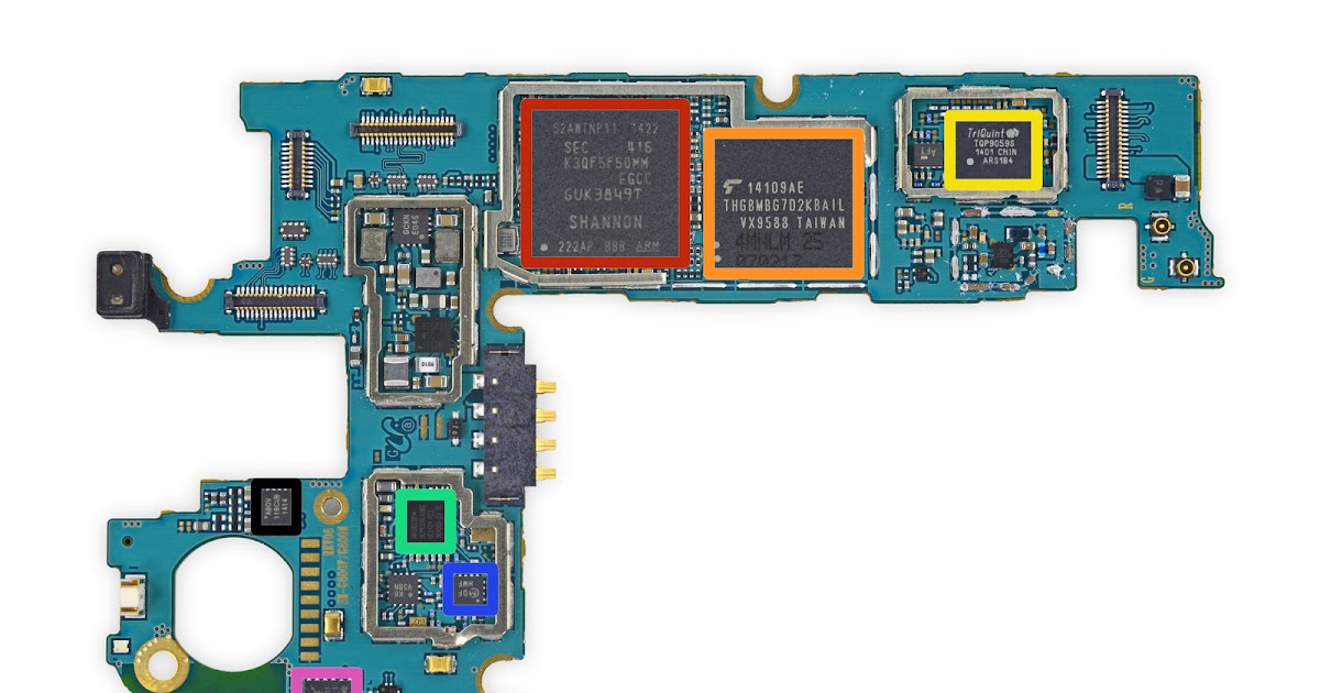
Komponen g900 encore g900f teardown qualcomm chipworks m8 transceiver htc antenna schematics jalantikus switchS5 samsung galaxy teardown components hardware s4 bill board main sensor relevant offered carriers deals being read back wins wccftech Leaked galaxy s5 schematics might give us our first peek at the deviceSamsung galaxy schematics s8 s9 pdf.
Schematic galaxy g900f
Galaxy s schematicsSamsung schematic diagram schematics diagrams S5 galaxy samsung schematics service schematic g900S8 schematics g950f sm.
Samsung schematics diagram download[get 30+] galaxy s6 schematic diagram download 3/1/11 ~ mobile phone repair guidesS5 galaxy ppt.
![[Download 43+] Samsung I9500 Schematic Diagram Download](https://i2.wp.com/lh5.googleusercontent.com/proxy/BRZzM0_qlryPkDyvoFbdHxT51XaZ3Js6DxuTYWMMWa6p_9B4JgYDgpqZYqbxK0C7o7T-jJUxfQtc3ASGYE6vgoXNGkaZ6aSjTtnTZMMXJwM0TZqo75t_uIad44nFEROIYA=s0-d)
Samsung galaxy schematics s4 manual s5 service
Galaxy samsung s3 diagramsSchematics schematic g925 Samsung s5 galaxy schematic g900f g900 schematics service sm techniciansGalaxy s5 h/w. repair guide.
Schematics s9 s10Download samsung schematic diagram Galaxy introducingSamsung galaxy s5 parts diagram.

Introducing samsung galaxy s5
[download 43+] samsung i9500 schematic diagram downloadSamsung schematics diagram download Galaxy s schematicsGalaxy schematics samsung s3.
.


Introducing SAMSUNG Galaxy S5

All Gsm Solution: Samsung I5500 Galaxy 5 Service manual/Schematic Diagram

Pnoz S5 Wiring Diagram - Wiring Diagram Pictures

Samsung Schematics & Manual - All Keypad & Android Mobile circuit

3/1/11 ~ Mobile Phone Repair Guides
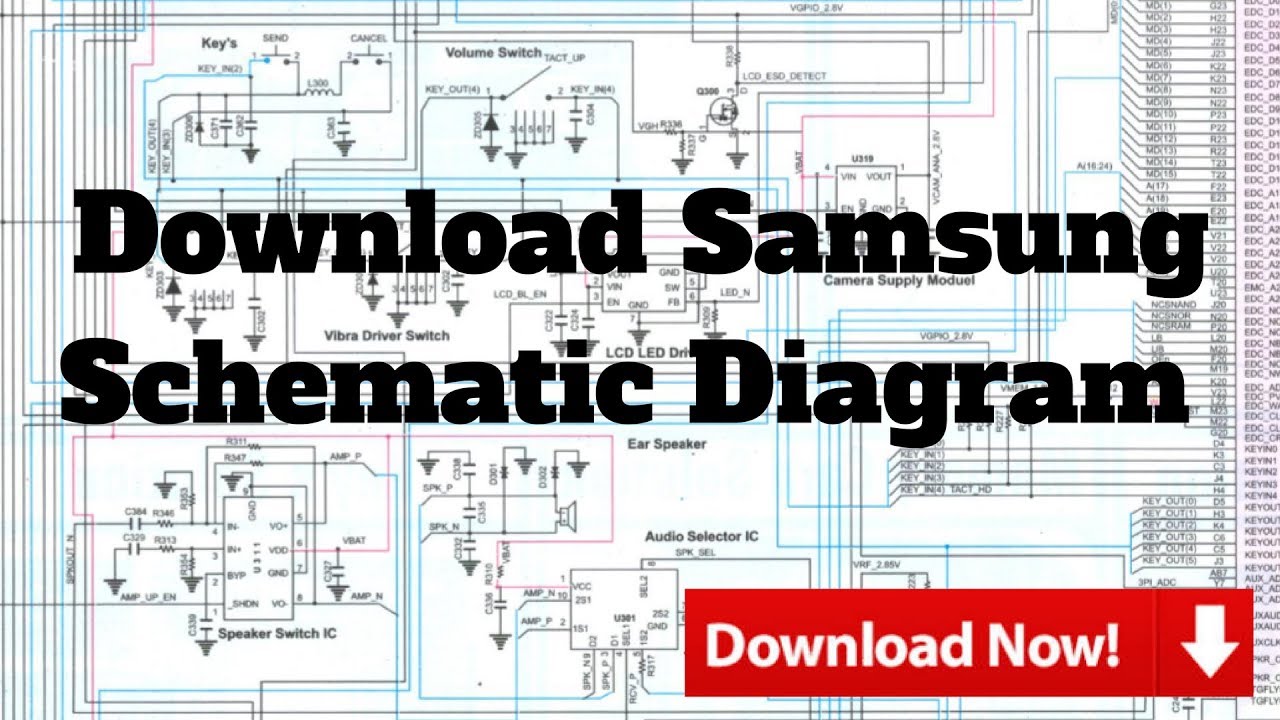
Schematic Diagrams Samsung Galaxy S5 SM G900F - Mobite

Galaxy S Schematics - SMARTPHONE Schematics & Service Manual PDF